Tooling tooling tooling. FPGA hardware is cool but the tooling fucking sucks. Like stepping back into the time where you needed to pay thousands of dollars to get decent compilers and debuggers.
The ability for anyone to develop software for CPUs at zero-cost is an amazing freedom. You literally cannot do that on certain fpgas--not only do they cost thousands, so do the tools to actually create a working design.
FPGA's are extremely powerful, but the toolchain is absolute dog shit. Xilinx, shame on you. Intel, will you change anything here?
The compound problem of this in reality is that finding the right people who have the right strain of semi-insanity to do this really well, is very slim. And most of them are tied up with a massive salary from some aerospace company such as Raytheon, GE, Honeywell, or someone like Philips (building medical devices).
Add to that compile times of an hour or a day, and you have a glacial development cycle on your hands.
HFT also still pays top dollar for competent FPGA developers. I'd wager they're willing to pay more than the listed industries too, especially if you factor in profit sharing and bonus structures.
1. The optimization problems that EDA tools have to solve are about as hard as it gets - NP-hard and sigma 2p problems at a massive scale. I'd argue that these are among the hardest optimization problems in modern computer science today.
2. The number of people with the CS + EE training to develop this software is decreasing. Not a lot of people are getting PhDs in EDA anymore, because:
3. Regular software houses (Google, Amazon, etc.) have about 2-3x the comp as EDA companies. Trust me I've seen a lot of incredibly smart EDA people jump to Google and more than double their salary overnight.
I doubt Intel is going to shift the balance here. It's not easy to develop a fast and efficient SP&R flow.
You know, we would all like faster synthesize and P&R cycles, but when people complain about the tooling being shit, that's not what they're complaining about. (Mostly)
C (or really any traditional programming language) doesn't really map to an FPGA. There are some compilers out there that attempt to convert traditional C code to state machines for FPGAs, but FPGAs are really a completely different paradigm. You're actually describing digital logic, not a sequence of steps.
That being said, there are soft-processors that have been written in VHDL/Verilog and can be incorporated into a FPGA design, and those CPUs do often have GCC support (Microblaze Xilinx, NIOS 2 Altera, plenty of MIPS CPUs out there, etc.).
Oh that's not what I was implying, sorry for the confusion. I meant an open source, portable HDL compiler/synthesizer like what GCC/LLVM are for software. As the parent and many others point out in this thread the tooling is a really sore point for FPGA development. It's always big, clunky, often buggy closed source applications (often running on an unhealthy dose of Tcl scripts cobbled together).
And of course if you change supplier you have to relearn everything or pay for an other third-party closed source solution to abstract some of the differences between the environments of Xilinx, Altera/IntelFPGA and friends.
Understood, and I totally agree that it is an industry ready for some shakeup.
I used to work for a large defense contractor doing FPGA work, and we really went out of our way to try to stick to 100% VHDL to attempt to avoid vendor lock-in. This meant things like writing block ram HDL in a way that it would be inferred by the synthesis tool to use the block ram (and not synthesize out of a bunch of LUTs).
It was a constant struggle to keep things synthesizing correctly. We mostly standardized on using Synopsys Synplify Pro for vendor-neutral synthesis and then using the Altera/Xilinx backend tools for place and route, etc. But even then, we regularly had to whitelist certain good versions of Synopsis' tools.
It was possible to do this with the vendor-specific synthesis tools too, but it was still a massive effort to check that primitives synthesized into the correct elements across different parts/vendors. Ugh, do not miss it.
The sore point of FPGA development is that not only the tooling is beyond terrible, it's also effectively a strong lock in. Changing designs is all but easy, even IF your design is not tied to specific hard fabric on the FPGA.
So you got terrible tooling and then a lock in into that tooling.
Not very appealing. Why the f--- would anyone use FPGA's unless they're the only option?
Last time I checked out Christiaan Baaji's CLASH, it was a Haskell DSL for generating RTL. That is neat, but it doesn't involve any LLVM-like abstraction of FPGA primitives for synthesis.
That would be more than neat, revolutionary really. But it would require buy-in from the major vendors, in the form of publishing many low-level device details.
Lattice has gotten some great product placement with recent parts. They have one that is cheap and essential to implementing voice command wake (siri, ok Google). Fpga have huge value for the right applications, but are often low value for individual developers since bring up time is so long.
The big consumers of FPGAs don't care if the tooling is terrible, because they're coming from 80s development environments and practices and can afford to dedicate 50-person teams to the job function.
Smaller companies won't touch it because it's terrible, and the vendors won't improve it because there's no demonstrated market for improvements.
Sounds about right. I guess the market economics don't work out for a simple design (i.e. with not much IP revealed by open sourcing the spec) that can be programmed with OS tools. I mean, there's these ICE chips, which is a huge step, but realistically I'd want something just a tiny bit bigger and with a hardcore (ARM or MIPS) in it.
Or maybe the market economics work out, but are small relatively compared to the big players, so it moves glacially.
The biggest problem with reconfigurable computing is it's either an afterthought, tools are too narrow/proprietary or an extra add-in card.
Add a million LUTs and several thousand special-purpose blocks (ALUs, CAM, SRAM, DSPs, etc.) on CPU die that can be reconfigured within a few 10k cycles (ie process context), and then future AI-enabled optimizing compilers could incrementally profile and accelerate applications with reconfigurable resources in new, creative and interesting ways. IRAM and similar zillion core approaches are another approach to solve traditional performance locality bottlenecks: distribute processing, interconnect and RAM amongst each other. It makes the most sense to co-evolve such a radical undertaking gradually with compiler vendors and large customers so that support and usability is working from launch, rather than just throwing silicon over the wall and using the "hail mary" method of product (non)design.
PS: Intel could push almost any new on-die CPU technology service/product into the mainstream right now on the server side because of their de-facto monopoly oligopoly dominance. I don't think they will as there is immense organizational pressure to not innovate too much.
> Add a million LUTs and several thousand special-purpose blocks (ALUs, CAM, SRAM, DSPs, etc.) on CPU die that can be reconfigured within a few 10k cycles
LUTs are implemented as a cascade of muxes that are controlled by local latches that are set at configuration time through a scan chain. Scan chains are key to letting you configure all these LUT control latches across the whole chip in an area-efficient manner, but there's a severe time vs area trade-off since you're essentially configuring one LUT control bit (a vanilla 6-LUT has 2^6 = 64 control bits) per scan chain cycle per scan chain. FPGAs already suffer ~30x area overhead for LUT logic compared to equivalent ASICs, so adding a lot of additional area to enable much faster reconfiguration seems like a tough sell. Matrix addressing as used in DRAMs and LED/LCD displays is another sweet spot on the time vs area trade-off curve. Not sure if anyone's ever done an FPGA using that as the configuration topology, but it'd probably make a fun dissertation topic.
There needs to be a marrying of software and hardware -- and processor instructions to support that. This is hierarchical reconfigurable cache-based architecture I designed a while ago at Intel; I doubt they have touched it but they do own it.
It's still terrible opsec. Of course, as always, it depends on the threat model. Still, linkage and contamination are deadly - why give up more information than absolutely necessary for your adversar[y|ies] to use against you in the future. All it takes is one mistake or a few 'almost mistakes'.
Yes, I've evaluated some of them too (great for some projects that need like a RPi but with custom digital / DSP logic), they're just not exactly mainstream as Xeon processors.
I have only used the original Xilinx one but ARM is pretty mainstream, the newest ones even have Mali GPUs.
I would expect a Xeon+FPGA to be at a very different price point from the ARM+FPGA devices, it will be interesting to see whether Intel carry on selling ARM ones or also produce an Atom+FPGA equivalent.
Not really. FPGAs tend to be accompanied by a flash memory storing the firmware, which of course has limited erase cycles, but you can also upload the firmware through other means.
The configuration is held in SRAM cells in most FPGAs. Like the other commentor states, the SRAM can be loaded in different ways, some of which have write cycle limitations.
If they do release something in this space they oughta make a SKU that can plop into a standard desktop socket on a standard motherboard.
Electrical and computer engineering individuals want cheap big FPGAs too! (Speaking for myself of course.)
Or just release a cheap pcie card! Cmon guys! Oh wait you've forgotten how important it is to get a developer community started around your hardware cause it's been so long since the x86 was new!
> Oh wait you've forgotten how important it is to get a developer community started around your hardware cause it's been so long since the x86 was new!
Intel: Huh? Developers? But they don't buy servers full of chips. Why do I have to sell to developers?
That is pretty much the ARM and POWER problem too, they think they can grow in new markets with these hugely expensive machines in quantities of ten racks.
Both would have significantly more traction if they offered a reasonable desktop class machine, but they don't seem to be able to do it. For some reason there are dozens of RPi type devices but making a $200-$300 device with a reasonable set of expansion ports (sata+USB3+pcie gen3+m.2+10g ethernet+etc) seems all but impossible. POWER has a similar problem, with the only inexpensive devices being old NXP parts (yah NXP is still selling a core that turns 20 years old this year https://www.nxp.com/products/microcontrollers-and-processors... thats great if your still selling car parts from 20 years ago, not so great if your designing a part today.).
The underlying problem here is that the cost of making an SoC is enormous. So to make, say, an ARM desktop class machine you have only a few choices:
1) Make your own SoC designed for the purpose. You can tailor it to meet your requirements precisely, but given the low volumes you'll be selling, your system will be at least $10,000 a box, likely more.
2) Use a designed-for-mobile SoC. This will hit your $200-$300 price point pretty easily (perhaps even sailing under it by a big margin), but the IO options will be bad, because mobile SoCs don't neeed SATA or PCIe. CPU performance is likely to be underwhelming because mobile SoCs are designed to hit a power consumption level that won't drain mobile batteries or make mobile devices overheat. Almost all the cheap devboards you can get today are in this category.
3) More recently we're starting to see server or networking SoCs, which gives you an option a bit like 2 but with different cost and expansion tradeoffs. Generally a bit more expensive than 2 because networking won't hit mobile volumes, but better I/O capability. CPU power may still be less than you might like. Examples here are the Macchiatobin board and the dev box that Socionext announced last week.
I don't think anybody disagrees that a proper desktop class machine for these architectures would be great; but there are huge economic barriers to getting there. Personally if I was looking at getting a new ARM setup I'd try something in class 2, likely the Socionext box when it becomes available (end of the year, I think they said).
Raptor Computing Systems will sell you a 4 core POWER9 CPU for $340 each [1]. A desktop mobo with the kinds of features discussed shouldn't be more than a few hundred dollars if slimmed down to one socket and a reasonable but limited set of peripherals (the Talos mobos go a bit over the top with features and hence are >$1k). Someone just has to design one, which is not easy or inexpensive, then hope that developers actually buy them.
It's a few hundred dollars if you have the market volume to sell it at that price. IBM have the volume (presumably mostly for servers) so they can do it. You can't spend the amount it costs to make a new SoC based only on the "hope" that people buy it; you need a business plan that says where the volume will come from, and there aren't enough customers for a developer box alone to provide that volume, so the dev box uses will always be a sideline from something else.
You can get lots of dev boards for existing SoCs. They have the problems of no PCIe, no SATA, etc that the n^parent was complaining about. If you want those features you first have to identify an SoC that has those; my claim is essentially that such pre-existing SoCs with the kind of features you want in a "developer box" are so thin on the ground as to be pretty nearly nonexistent. "Use a preexisting SoC" is what my classes 2 and 3 are.
Nah, the problem is the SOC mental model where you don't provide a generic IO bus. What ARM/etc really needs is a device with a decent memory and PCIe interface. Random board manufactures can then glue on the ethernet/sata/USB for a few bucks a function utilizing 3rd party chips that can be found on boards frequently costing less than $10.
That way instead of spending millions designing a SOC for each tier of devices you design a "generic" device and sell the ones with busted cores/cache/ram channels/whatever as low end developer machines after fusing the broken functionality off.
It's the lowest possible effort custom design you could make. The only major difference between the three generations of Pi SoCs (BCM2835, 2836, 2837) is the CPU, so it's a 5 year old SoC designed for set top boxes with a single IP block swapped out.
That may be true, but its the 1 huge customer vs a million little ones problem. Sure when you win the hyperscaler contract you hit the jackpot, but OTOH, when you don't you go out of businesses. Having a few thousand developers testing/optimizing/etc compilers/OSs/databases/web servers/etc all make it easier to win the hyperscaler contract, than spending months wondering why docker doesn't run correctly and loosing the contract.
So, a company may only be making a dollar on each machine sold, but is gaining thousands of hours of beta testing, or actual engineering in return.
I should add though, that this months basement hacker is next years businessman buying in lots of 5k to fulfill some small niche market. Do that enough times and eventually the next netflix/facebook app just happens to be running on your hardware.
The whole things smells like monopoly dragging its heels. It bought the competition to slow adoption, claiming that CPU-FPGA hybrids were just around the corner. What we need is a new FPGA based fabric that has the major building blocks to create any number of RISCV cores. Tiles that can be RISCV, or if "sacrificed" turn into clusters of LABs for general purpose use. And the chip company with the software vision for this is AMD with HSAIL.
FPGA's are the shit but the software is the key. To make them really fly we need some really brilliant software to configure them. Someone is going to disrupt this space soon and whoever does I think will make a unicorn. Just my guess.
They bought one of the best hardware makers with one of the worst software platforms. I hope to all that is holy that they replaced the software entirely. What a nightmare those classes were...
What I am interested in is a programmable vector fabric that I can reconfigure fast (in say L2/L3 access times). right now there are 100s of AVX2 instructions & as the number of HPC applications grow it is only going to explode. My problem is that when you are using one vector instruction the silicon for the rest is just sitting around when it could be perhaps used to make a much wider SIMD unit for just the instructions I'll be using. If they can get just that right IMO it'll be a huge success.
IMO the problem with FPGA or even silicon dev is mostly tooling. I often say this, the biggest contribution to Open SOurce movement is not of linus/linux ..its gcc. just imagine if 'they' could tangle up every bit of open source code in IP litigation emerging from proprietary compilers.
The applications are the same, but an FPGA allows extremely narrow optimization. Got something that doesn't parallelize all that well, but can be pipelined, or benefits from a wide datapath? Design that. Got something that parallelizes well and only needs a tiny datapath? Make it a 1000 wide vector machine. It needs difficult control flow? No problem, we're flexible as we're not a GPU, etc.
The optimization needs to beat out the inefficiency of the FPGA compared to an ASIC though (not to speak of development time). But sometimes, you can do just that.
I have worked on this in the case of Smalltalk and the opportunities are there but there are significant problems. The opportunity is in the form of adaptive compilation where you initially use a simple compiler (or even an interpreter for the very first execution) and then collect profiling information and call a much better compiler to generate code for the "hot spots". A key optimization is inlining which greatly increases the size of a basic block. You could add a third step for the really, really hot spots and compile to hardware.
With commercial FPGAs you have a problem that you can't generate the bits yourself but have to use the vendor tools. These are pretty simplistic and will take minutes or hours to compile non trivial circuits. What I mean by this is that they flatten the netlist at some point so compilation time grows non linearly with circuit size. So if your design has five identical blocks, adding a sixth might make it take twice as long to compile.
A second problem is that it takes a while to load the bits into the FPGA. The old XC6000 could be accessed as RAM and quickly rewritten but all other models serially shift in the configuration bits. Xilinx allows partial reconfiguration where you can load the bits to one part of the FPGA while the rest continues to work but that is pretty hard to use and the competitors don't even offer this option.
I'm sure I missed something in your first paragraph though, because the process that you described sounds very much like a normal modern JIT compiler. In V8 and SpiderMonkey for example, the engine starts with the first tier, which is a baseline interpreter that collects type information on each function call, and then if a function is invoked enough times, it compiles the function to machine code using the type information collected in the first tier. There are more tiers up the chain, slower to compile and faster to run, where dataflow analysis is done on the hottest functions, which get optimisations such as inline caching, etc.
All that is done on the CPU of course, so I'm curious how an FPGA could help in this process?
JIT is a generic term that applies both to dynamic compilation (one pass) and adaptive compilation (multiple passes with profiling). While it is pretty normal these days, many people involved in FPGA research only know about static languages and manual partitioning (like OpenCL) and that is why I always explain what it is.
FPGAs don't help JITs at all. I was saying the opposite: if certain problems (slow compilation and slow reconfiguration) could be solved then JITs could offer the opportunity to generate hardware acceleration on demand that would be tuned for a specific execution of an application.
The problem is that tailor-made FPGA designs won't run nearly as fast as a modern ASIC CPU. That's why for instance FPGA emulators are not more common, for older hardware software implementations are accurate enough and manage to run in realtime so the additional cost and complexity of FPGAs is not warranted.
For more modern hardware software implementations can't reach absolute accuracy in real time but FPGAs big and fast enough to handle these designs are prohibitively expensive (if they even exist in the first place). That's why FPGA GameBoy emulators are not popular and you probably won't see a FPGA PS3 emulator any time soon (unless the pricing changes dramatically in the near future).
FPGAs shine when you need to process very high throughput data with low (or at least constant) latency or for special-purpose algorithm with no hardware acceleration available on CPU or GPU (video codecs, crypto, computer vision etc...). But in general when an algorithm becomes popular enough (AES, SHA-256, H264...) hardware support is backed into the ASIC eventually with much better performance and power consumption than a FPGA.
I see a potential for FPGAs in CPUs for professional applications if you want to process big datastream without having to rely on external hardware. For instance I work in broadcast video transmission where we routinely handle uncompressed HD or even 4K streams, being able to prototype directly on my workstation's CPU would be pretty cool.
As for general purpose programing language optimization I have a hard time imagining what it would look like. The problem is that you don't code for a FPGA the way you code for a CPU. To put it very simply on the CPU serial is cheap while forking and synchronizing threads is expensive. On an FPGA it's basically the other way around. Automatically transforming one form into the other automatically in a compiler or JIT sounds very much non-trivial. Maybe I just don't have enough imagination.
I'm kind of fascinated by any type of accelerator chip for some reason - I think it has something to do with the design of the computers I had when I was a kid i.e. Spectrum, Amiga etc which had dedicated chips for particular facets of the functioning that became iconic. I would love to do something with FPGAs and am certain their potential is massive, but struggle to come up with a use case that seems in any way novel, and I don't really want to just build my own VGA controller, get bored, and stop there!
I remember a talk by Alan Kay where he mentioned a number of problems commonly solved serially, such as 2D layout and typesetting, and then he demonstrated a parallel algorithm for each problem. If I remember and understand correctly (I may not), one of his points was that such algorithms can become trivially implementable in a dynamic language and would run fast too, if the hardware supported some of the primitives of that dynamic language natively. He expressed hope that FPGAs may create such an opportunity.
Alan Kay gave a talk at Qualcomm in San Diego, on October 30, 2013.
"Is it really complex or did we just make it complicated?" https://vimeo.com/82301919
The common sentiment after the 90's is that it's hard to beat optimized x86 implementation of both. Maybe non-offloading FPGA-CPU hardware has the potential of accelerating certain language features (e.g. burn in the CLOS method lookup cache?)
Yes, you do need the vendor's place-and-route. PAR performance is as good as you could expect though.
Most complaints about vendor software are closer to the front of the flow. Examples...
* Poor language support (applies for both SystemVerilog and VHDL)
* Not enough transparency and access to primitives and IP blocks, resulting in poor ability to automate
* Generally buggy elaboration and synthesis results, sometimes even causing the tool to crash
My opinion is that the FPGA companies spend too much money improving the HLS (c-to-gates) and IP wizard experience, in an attempt to make their devices more accessible to the mythical software engineer who wants to use an FPGA.
They should have spent that time and money supporting language standards, and improving the RTL experience, which is how most engineers use their products.
It sounds like it would be little different from a CPU implemented on an FPGA. True, you want to use run-time info to optimize on the fly, but my guess is that modern branch predictors, caches etc, already do as much of this stuff as we know how to do.
In the unforseeable future, then who knows, maybe the predictors will become so flexible that even conventional CPUs evolve into something like basically FPGAs.
I've honestly been waiting for this since for YEARS.
I've had a vision for "the future of computing". FPGAs that reconfigure themselves (<-these exist) to become whatever macro-level hardware assets your computer needs. Running tons of SHA-256 encryptions per second? The CPU/OS/OpenSSL (or whatever) detects this condition and switches from hand-coded ones, to an IP core that comes with the CPU. The CPU flashes the FPGA's to become SHA-256 "CoreS" and now you're running 4096x the output with less heat. (As CPUs are designed for one thing "few, large, complex cases" while FPGAs are perfect for many, parallel simple cases" even more than a GPU.) Now, you shutdown your encoding and switch to video encoding, or Doom 2019 and your CPU reflashes (Alteria specialized in PARTIALLY flashable FPGAs so you don't have to nuke the entire FPGA, only sections) and adds cores for video, or physics, or "shader units".
This would be hard for a single person, but any large company could handle making this. You can even do it with off-the-shelf FPGAs. The biggest problems are 1) bandwidth. The "macro" function size needs to be bigger than the latency hit you take for asking the FPGA over computing it internally. (Intel's on-CPU FPGA would be insanely fast access.) and the other one is 2) How do you get people to use it! The simplist is of course, only supporting people who actually request it. But, you can take libraries that perform common, encapsulated macro functionality, like OpenGL, a physics library, or OpenSSL, where people don't care about the inner code ("how it gets done") but instead the result. Asking for floats to be multiplied would be bad. But asking for a cross-product would be much faster. Asking for an SHA-512 key would be super.
And the benefit here is, you don't have to hardcode that functionality into a CPU. The FPGA can have NEW or improved IP cores downloaded with Windows Update every week.
Back when I was in college, I actually bought a Lattice dev kit with a PCI Express card, dual-gigabit ethernet, DDR3, and an near top-of-the-line FPGA on the board and it cost a mere $100. Unfortunately, I was a more software guy so I really got in over my head (plus health issues set me back and have never let up since), so I never got a working prototype built.
But it's still there! A huge opportunity waiting to be seized that could really become another tier of "the standard PC." In the same way we think of SSDs as "almost RAM" scratchpads, or GPUs as "CPUs for massive amounts of simple decisions." Well an FPGA is the "GPU of GPUs". Even simpler decisions and insanely fast and parallel even at "low" (by CPU standard) clockrates of 400 MHz.
Here's an older (2009) project/research article that inspired me called the 512 FPGA cube.
Those are massive differences in numbers in both power efficiency and compute rate. 72,000 Watts of Xeons to get the speed of a single 832 watt cube. That's two orders-of-a-magnitude!
I mean, imagine a world if they bothered to make FPGA's you could plug into Ethernet, and make them configure themselves according to a simple programming tool that was "easy" for normal programmers to exploit instead of requiring intense understanding of logic gates, propagation delay, and so on. A tool that wasn't "as fast as" a dedicated engineer, but 90% (or even 70%) as fast at zero cost and effort. All a sudden you could run tons of programs and macro-sized functions like you had personally stamped them into a printed circuit yourself, but without spending millions on development.
I'm honestly not sure why this hasn't already happened. I can't be the only "smart" person who came up with this idea. And the research (and practice with bitcoin miners) all points to a huge opportunity to be exploited if they could lower the knowledge barrier-to-entry so you can basically "push a button" and unleash an FPGA at a problem. Imagine LAPACK and BLAS with FPGA support.
It just doesn't deliver on performance, or energy consumption. That was always going to be the case (you are adding a layer of abstraction at the silicon level). So for anything that is measured on "operations / second" or "operations / joule", FPGAs will always lose out. By now industry has learned that the key is to tailor algorithms for what we can do fast (vector+branching on CPU, everything branchless on GPU), not shoehorn silicon into algorithms.
So what can FPGA do? Fast, low latency, high bandwidth interaction with peripherals. The irony here is that to have this work out, you kind of want to have your peripheral connected to the FPGA.. which takes away all the fun from the reconfigurable stuff, because you can't reroute your PCB. So now 99% of FPGAs deployed end up running in the same configuration always and companies with the necessary scales pour it into ASICs.
FPGAs solve a niche problem of interacting with very fast, massively parallel data buses and systems (think CCD sensors, ADC sampling, ..) that a linear execution, Turing style processor isn't suitable for. And pretty much only for applications where you don't have the volume to convince a chip manufacturer to put your peripheral into silicon.
> As CPUs are designed for one thing "few, large, complex cases" while FPGAs are perfect for many, parallel simple cases" even more than a GPU.
FPGAs are quite good at parallel simple cases, that is correct, but they would lose to GPUs in performance/watt in most cases.
Where FPGAs really shine is in parallel complex, non-uniform cases, especially cases that don’t map well to the classic CPU instructions, but can easily be performed with small latency on FPGAs.
FPGAs own low latency computation (less than 1 microsecond) because GPUs really need 3-20 microseconds to initialize after a kernel launch. This is why they're used instead of GPUs at the front line of high frequency trading. When I was at a hedge fund, I tried in vain to get Nvidia to do something about this based on the unofficial work of another former Nvidia employee implying this could be improved dramatically.
All that said, these are golden years to be a low-level programmer who understands parallel algorithms whether you work in Tech or at a hedge fund because there just aren't that many of us.
But the real problem with FPGAs is that even if they find another lucrative application where they excel relative to GPUs, Nvidia can simply dedicate transistors in their next GPU family to erasing that advantage as they did with 8-bit and 16-bit MAD instructions in Pascal and with the tensor cores in Volta. Too bad they don't care about latency or I believe they could disrupt FPGAs from HFT in a year or two when someone started using them and started winning.
Especially if the level of parallelism isn't too large, or if the memory bw requirement for each is low. The memory bandwidth of FPGAs is comically small typically compared to GPUs if it has to go to off-chip memory. Internal memory is limited to a couple MBit typically.
0) Trying to do automatic parallelization is something we've been working on for 50 years and we still haven't solved in any practical degree. You can't just slap a #pragma on C/C++ code at this point to say "run this on some non-CPU architecture" and expect to get good performance.
this (or something very close to this) has been described in 1993 (!) paper/article called 'processor reconfiguration through instruction set metamorphosis' or PRISM.
perhaps you might find it interesting. have fun :)
I've been thinking of something similar recently - to extend your idea slightly, why couldn't the flashing of the FPGA happen per tick? Thus at every tick your FPGA could become entirely different hardware, tailored to whatever task is required at that tick.
Well, flashing is pretty slow compared to modern computers. You have to load it from flash (no pun) memory and Altera are the only ones (AFAIK) that support only changing subsections. (Which could be great because you can change only a half or quarter of your FPGA with new logic units while the others keep running.)
Also, you'd have to know what you'd need... before you need it. Which is kind of impossible. By time you know you need tons of integer units, you probably could have started working on them. That is, if you need to rapidly switch, then your workload is pretty rapidly completed to begin with.
However, I don't thing they need to reconfigure that fast. Once every second would be enough to keep up with most workloads. Most "heavy duty" workloads aren't changing that rapidly. You load a video game, it's a videogame for hours you play it. You load a web server, you're going to be doing SSL.
If you need much more fine control, it'd probably be better to treat the problem at a much higher level ("I need more SSL keys / sec", instead of "I need more integer adds to make SSL keys") or add another FPGA (one for each use case or set of use cases, ala one for web server keys, one for deciding some other major web server feature).
Of course, I'm no expert in the field. I'm just a guy with an idea and some experience / research into FPGA's as reconfigurable logic units.
Yes, it's the predictive aspect of it that I've struggled with also! I understand there are technical limitations at present, was just trying to extend the idea beyond what's currently possible to see if it might be interesting.
> CPUs are designed for one thing "few, large, complex cases" while FPGAs are perfect for "many, parallel simple cases" even more than a GPU
<offtopic>Hmm, where have I heard something like this before ... ah, yes, the brain - CPUs/FPGAs are like reason and instinct, because reason deals with "few, large, complex cases" and instinct has "many, parallel simple cases". The brain has its own CPU/FPGA divide.</>
Wow that is a solid plan. I propose you or whomever builds it calls is Nitro or something to that affect. Speed how you need it. Imagine an open library or FPGA profiles for popular apps. Build one for Photoshop and you have yourself a nice biz.
If they ever release it in the first place (or if they ever let it get past a point where you need to specifically contract with intel to get access to it).
This is so obviously not going to fly unless they either start bundling with Xeons, or offer something Xilinx can’t do. Cloud providers aren’t stupid, and there are enough eggs in the Intel basket already.
One of the key benefits of Intel's solution is that the CPU and FPGA share the same RAM, avoiding the O(N) cost of moving data to/from the devices. This type of a zero-copy transaction can enable very high performance applications compared with dedicated discrete cards.
AMD already does "Zero Copy transfers" (the on-chip cache!!) with its "Fusion" APUs (ex: A10-7850K) for CPU <<---->> GPU.
I'm not really seeing loads of people taking advantage of the feature however. The platform is cheap, the technology is available but its just way too weird an architecture to become mainstream.
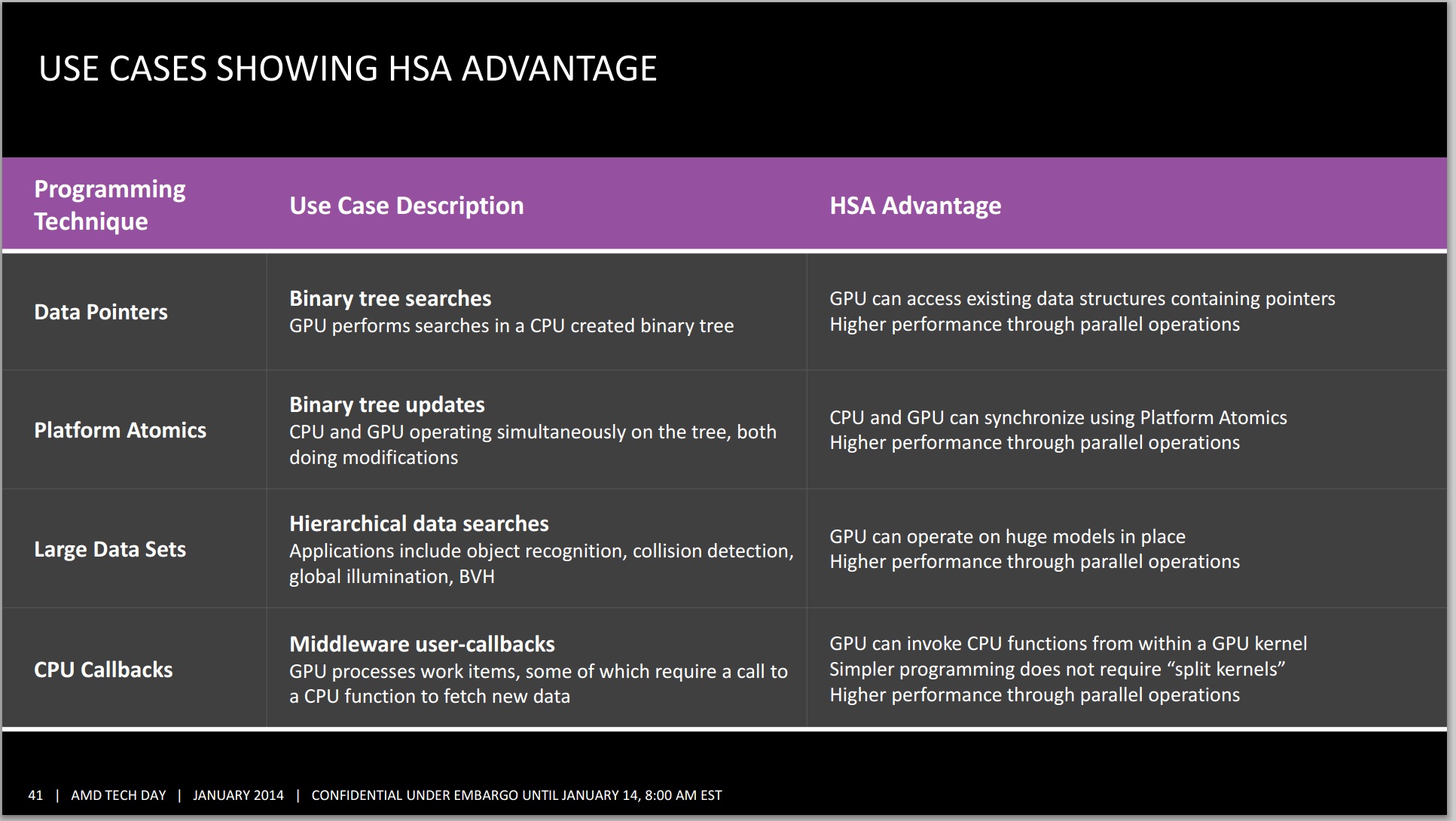
There are numerous benefits: the CPU can create a linked list or graph, and the memory will still be valid on the GPU. CPU / GPU atomics are unified, and GPUs can even call CPU functions under AMD's HSA platform.
I think Intel had a similar technology implemented on their "Crystalwell" chips, which were basically an L4 cache which provided a high-bandwidth link between the CPU and GPU (although not quite as flexible).
No, its not an FPGA, but OpenCL / GPGPU compute seems to be a bit more mainstream than FPGA compute at the moment. I haven't seen too much excitement in general for this feature however.
>I'm not really seeing loads of people taking advantage of the feature however. The platform is cheap, the technology is available but its just way too weird an architecture to become mainstream.
AMD sells a consumer product. For most consumers even a smartphone offers enough CPU and GPU performance. The content producers who care about performance usually buy the best CPU and GPU. HSA isn't available on AMD's Ryzen or Threadripper processors.
Intel is trying to sell to datacenters where performance or energy efficiency is a major selling point.
> The content producers who care about performance usually buy the best CPU and GPU. HSA isn't available on AMD's Ryzen or Threadripper processors.
Raven Ridge will be based on Zen CPU cores and Vega GPU cores. But naturally, Raven Ridge will be slower than Threadripper because the GPU will take up some space (that otherwise would have been additional CPU cores).
Rumored specs of Raven Ridge APU is 4 CPU cores and 11 GPU Compute Units. In contrast, Threadripper is around 16 CPU Cores and Vega 64 is 64 GPU cores, separated by a PCIe x16.
So basically, its the price you pay for sticking so many things onto a single package. There are thermal limits, as well as manufacturing limits (ie: practical yield sizes) to how large these chips can be.
If you want the best of both worlds, like an EPYC CPU with Vega 64 or a high-end NVidia Pascal / Volta chip, you'll need to buy a dedicated GPU and a dedicated CPU. True, a hybrid chip like Raven Ridge (or any of the AMD HSA stuff) has benefits with regards to communication, but the penalty to CPU speed and/or GPU speed seems to be huge.
-----------
I personally expect that if any "mainstream" FPGA solutions come out, they'll be connected to the PCIe and not merged into the CPU. There seems to be just too many heat and manufacturing issues to make a merged product compared to the standard PCIe x16, which is quite fast.
Alternatively, certain tasks (like Cryptography) can be accelerated using dedicated instructions, like the Intel AES-NI instruction set. Or Intel's Quicksync H.264 encoding solution. Fully Dedicated chipspace (like AES-NI) is way faster and more power efficient than FPGAs after all.
Idunno, Xeon Phi, their GPUs since about 2007 (though a lot better recently), good cooperation and documentation with their NICs, direct participation in both major open compiler toolchains, all the stuff that 01.org lists... I think they're doing pretty well with open (aside from the products themselves, but that's kinda the point of having a company).
Frankly Intel has done an adequate to good job of providing open source software to interact with all of their hardware for as long as I've been computering. They're the one vendor that has never told me to install a proprietary driver.
Intel really don't do anything unless they already have a market for it. They have bundled with Xeons in the past.
If there turns out to be a market (which comes down to tools and cloud platform to make this existing tech much more accessible) then it'll be huge and they'll need to be part of it.
The ability for anyone to develop software for CPUs at zero-cost is an amazing freedom. You literally cannot do that on certain fpgas--not only do they cost thousands, so do the tools to actually create a working design.
Until that changes, FPGAs will always be niche.